1. Paper
Writing ideas onto paper is certainly not a new phenomenon, however, it is surprisingly not that old. After paper was invented around 100BCE by the Han Dynasty, emperor Ho-Ti started the world’s first paper industry. This rudimentary form of paper was made from mulberry bark hemp rags, and water. The pulp was mashed into a flat patty before being dried in the sun.
Chinese paper improved literacy rates, spread religion through scrolls and books, and created banknotes that absorbed ink for permanent and counterfeit-free transactions.

2. Optical Lenses (glasses)
A lens is a transparent material that disperses light beams by means of refraction. Depending on the type of lens, an optical lens can be used to start fires (burning-glass), illuminate a room, correct vision, and more. The oldest discovered optical lens dates back to 2700BCE in ancient Assyria and was likely used as a magnifying glass or a burning-glass. Now modern lenses are used to concentrate light in eyewear, lasers, microwaves, microscopes, projectors, lighting, and telescopes.

3. Concrete (cement)
Concrete was originally developed by the Romans and became a widely popular architectural material by about 150BCE. The Romans used an aggregate and hydraulic mortar and gypsum or lime cement that hardened over time, even in water. Their advanced mixture was used to build incredible structures such as The Pantheon and The Colosseum in Rome. When the Roman Empire fell, modern concrete uses steel girders to form a rigid superstructure, however the ‘recipe’ for concrete has not changed drastically from the peak of Ancient Rome.

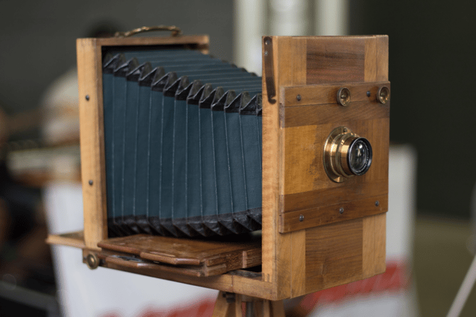
4. Photosensitive film (camera)
The earliest recorded photographic process was introduced in 1839 using light-sensitive chemicals formed on the surface of silver-plated copper. This process was replaced by thin glass plates coated with a photosensitive emulsion. Between 1885 and 1908, plastic replaced glass negatives before chemical photography became outmoded by digital photography 100 years later.
5. Tungsten (lightbulb)
Tungsten is a metal element that is used as an extreme conductor, dry lubricant, drill bits, jewelry, and military bullets. According to Live Science, it is one of the toughest things found in nature and is almost impossible to melt. It is resistant to corrosion and has the highest melting and highest tensile strength of any element. Because of its durability in high temperature environments, tungsten is traditionally used in incandescent light bulbs.
Tungsten was isolated in 1783 by Juan and Fausto Elhuyar however, more than 350 years ago, porcelain makers in China incorporated a unique peach colour into their designs by means of a tungsten pigment that was not known in the West.

6. Steel
The earliest known production of steel date back to 1800BCE, however it was not until the 17th century that the process was improved enough for commercialization. In 1855, the Bessemer process made steel stronger, less expensive, and produced in mass. The 1950s improved steelmaking by pumping oxygen directly into a furnace to decrease impurities. Today, steel is one of the most common building materials and has one of the highest recycling rate of any material at 60% worldwide.

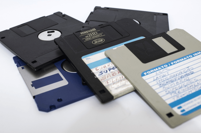
7. Floppy Disk
With the advent of personal computers, the floppy disk was essentially the first practical portable memory device. Floppy disks were invented in 1967 holding a total of 80 kilobytes of data and became the universal format for data transfer from the 1970s to the mid-1990s. Flash memory or USB drives became more practical beginning in the late 1990s and the floppy disk became outmoded as it was limited to a maximum of 2880 kilobytes in a 1992 release.
8. Touchscreens
The first touchscreen was conceptualized in 1965 and produced in 1982 for air traffic controllers. Up until 1988, touchscreens had a reputation for being imprecise until the common “lift off” strategy made it easier to select the intended part of the screen (the item would not be selected until the finger left the screen). Modern touchscreens, such as smartphones, use a transparent conductor called indium tin oxide (ITO)—derived from rare earth metals—that renders touchscreens rigid and brittle. These types of displays are called capacitive touchscreens and are widely used in smartphone applications.

9. Fiber Optic Cables
Fiber optic cables were originally developed for medical purposes in 1960, however they were not capable of traveling long distances. Fiber optics as we know them today were conceptualized by a man named Dr. Charles K. Kao by using fused silica. Today, more than 80% of all long-distance telecommunications are carried over optical-fiber cables.
Every time you browse the internet, you are interacting with an intricate network of fiber optic cables that not only span your country, but also entire oceans. If you have ever wondered how the internet spans oceans in seconds, check out these maps here.

10. Photovoltaic Solar Cells
The first residential photovoltaic solar panel was installed on a New York City roof in 1884. The cells were made with selenium and yielded a whopping 1% efficiency. The first electric solar power plants were developed in the 1980s but were criticized by inexpensive coal prices. Today, it costs less than 68 cents per watt of electricity produced via solar technology and panels can be up to about 30% efficient.
According to the Shockley-Queisser Efficiency Limit or SQ Limit, the maximum theoretical efficiency of a solar cell can be calculated under ideal conditions. These limits could actually be overcome by using nanotechnology to passively concentrate light from wide angles without using systems that track the sun. Nanotechnology infused solar panels can create a new class of solar panels that would be ideal for harvesting energy in the transportation and aviation industries.

11. Metamaterials
Imagine a new type of machine that is smaller than the unaided eye can detect. This is the goal for some new revolutionary optical smart materials such as those created by Metamaterial Technologies Inc. Metamaterials are a new class of material that usually uses nanotechnology to create nanostructures within common materials such as metals or plastics. The nano-structures within these materials are called “meta atoms” and can exhibit unique properties that conventional materials cannot. Smart materials therefore gain their properties not from their composition, but from their exactingly-designed structures that can be as small as 100nm thick—50 times smaller than the thickness of a human hair.
By creating metamaterials with specific nanostructures, metamaterials can achieve some remarkable effects. Some of these include blocking intense lights from damaging vision, improving solar panel absorption, and making lights significantly brighter without using electricity through a process called light extraction.

Learn more about the advancements in this incredible technology—Download About Metamaterials: Your Guide to Manipulating Light!